Products for PCBL™ Process
We offer products for various processes.
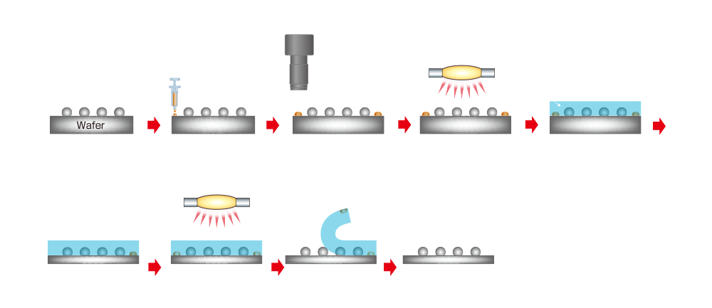
PCBL™ (Pattern Coating Before Lamination) Process
We propose a T.T.V. improvement process using dedicated equipment and UV resin for bump wafers.
To address the issue where the BG tape on the wafer edge without bumps dips after lamination, UV resin is applied to the wafer edge
to eliminate the step height, enabling improvements in T.T.V., grinding mark quality, and chucking reliability.
After back grinding, the UV resin can be removed together with Lintec’s UV‑curable surface protection BG tape (E series),
helping minimize the additional process load.
Suitable Equipment
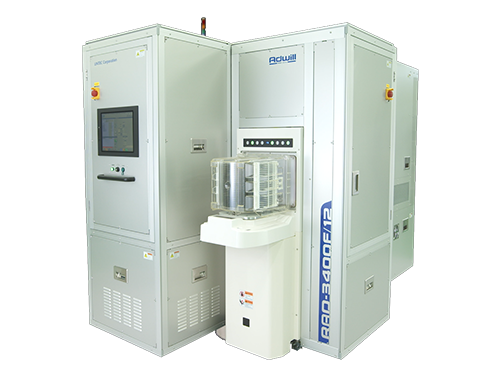 RAD-3400F/12 (UV resin pattern coater)
- RAD-3400F/12 (UV resin pattern coater)
-
Pattern Coat UV Resin Application Equipment
- 1.Compatible with 8‑inch and 12‑inch wafers
- 2.Equipped with an alignment mechanism
- 3.Equipped with resin coating and UV irradiation mechanisms
- 4.Capable of inline operation with the RAD‑3520F/12 (300 mm fully automated BG tape laminator)
Suitable Resin
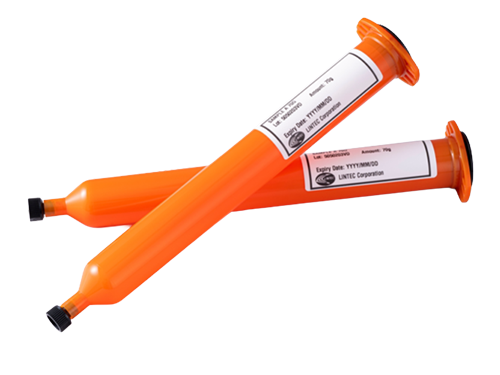 UV Resin for PCBL (CR Series)
- UV Resin for PCBL (CR Series)
-
UV curable resin
- 1.In‑house resin development
- 2.Resin supply optimized for required coating height and coating width
- 3.Back grinding can be performed after BG tape lamination
- 4.Removable together with BG tape
Suitable Tape
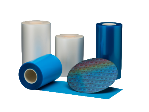 E series (UV Curable BG Tape)
- E series (UV Curable BG Tape)
-
The Adwill E series UV curable back grinding tape protects wafer surfaces and prevents contamination during the back grinding process.
Advantages of the PCBL™ Process for Bump Wafers
Conventionally, the tape on the areas of the wafer without bumps tend to dip, resulting in grinding to a thickness greater than the target thickness. When there is a large thickness difference between the wafer edge and the inner area after grinding , it can lead to cracking and grinding marks. By applying UV resin, tape dipping is eliminated, enabling improved T.T.V. and reduction of grinding marks.
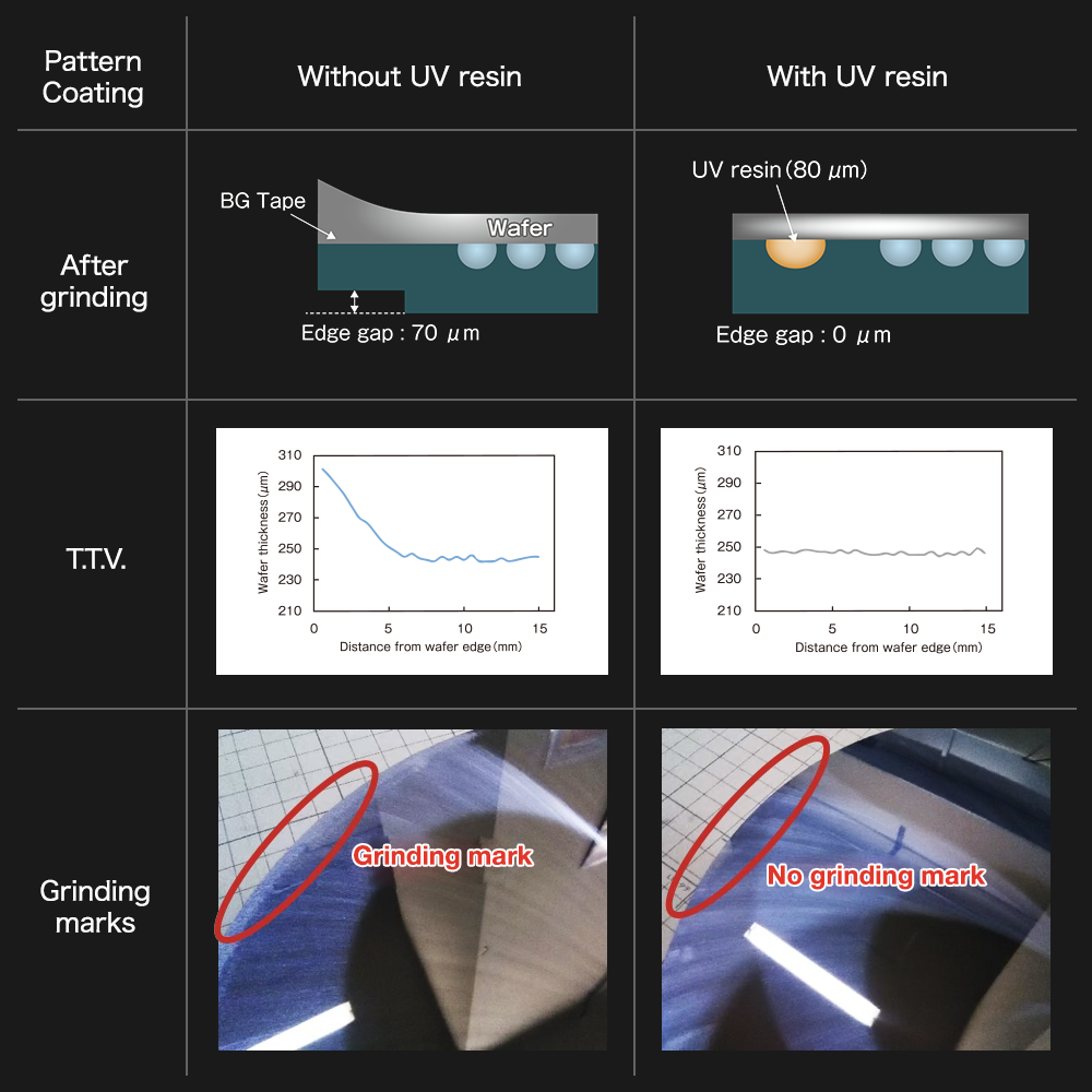
Evaluation Conditions
Wafer size: 12 inch, Bump height: 200 µm, Bump pitch: 400 µm, Target wafer thickness: 250 µm, BG tape: E-9486 (LINTEC)