
We offer various tapes.
BG Tape
 (UV Curable BG Tape)
For Standard Back Grinding Process
-Standard (>100 μm wafer)-
The indicated values are measured values and not intended for guarantee use.
| E-6142S(S) | E-6152B | E-6170(S) | ||
|---|---|---|---|---|
| Tape Thickness(μm) | 130 | 148 | 170 | |
| Appearance | Opaque | Blue | Opaque | |
| Structure | Base Film (μm) | PO 110 |
PO 108 |
PO 110 |
| Adhesive (μm) |
20 | 40 | 60 | |
| Adhesion*1 (mN/25 mm) |
Before UV | 5400 | 6740 | 11300 |
| After UV*2 | 55 | 50 | 55 | |
| Remark | Standard | Clear Blue (Transparent) | For Low Bump | |
*1 Peeling speed= 300 mm/min, Peeling angle= 180deg. Adherend: Si mirror wafer
*2:UV ray intensity: 230 mW/cm2, UV ray dosage 380 mJ/cm2 Wavelength of ultraviolet should be around 365 nm.
For Standard Back Grinding Process
-Thin Wafer (>40 μm wafer)-
The indicated values are measured values and not intended for guarantee use.
| E-8180HR | ||
|---|---|---|
| Tape Thickness(μm) | 180 | |
| Appearance | Blue | |
| Structure | Base Film (μm) | Special Elastomer 160 |
| Adhesive (μm) |
20 | |
| Adhesion*1 (mN/25 mm) |
Before UV | 5390 |
| After UV*2 | 250 | |
| Remark | Low Warpage | |
*1:Peeling speed= 300 mm/min, Peeling angle= 180deg., Adherend: Si mirror wafer
*2:UV ray intensity: 230 mW/cm2, UV ray dosage 380 mJ/cm2 Wavelength of ultraviolet should be around 365 nm.
For Standard Back Grinding Process
-Anti-ESD-
The indicated values are measured values and not intended for guarantee use.
| E-6130AS | E-3090V AS | ||
|---|---|---|---|
| Tape Thickness(μm) | 130 | 90 | |
| Appearance | Opaque | Blue | |
| Structure | Base Film (μm) | PO 110 |
PET Composite Film 80 |
| Adhesive (μm) |
20 | 10 | |
| Adhesion*1 (mN/25 mm) |
Before UV | 5700 | 11000 |
| After UV*2 | 55 | 30 | |
| Surface Resistivity*3 (Ω/□) |
Before UV | 1.0 x 10¹⁰ | 1.3 x 10¹⁰ |
| After UV*2 | 9.1 x 10¹² | 4.3 x 10¹² | |
| Remark | For DBG™ | ||
*1:Peeling speed= 300 mm/min, Peeling angle= 180deg. Adherend: Si mirror wafer
*2:UV ray intensity: 230 mW/cm2, UV ray dosage 380 mJ/cm2 Wavelength of ultraviolet should be around 365 nm.
*3:ADVANTEST DIGITAL ELECTROMETER R8252 ,Measurement : Adhesive side
For Standard Back Grinding Process
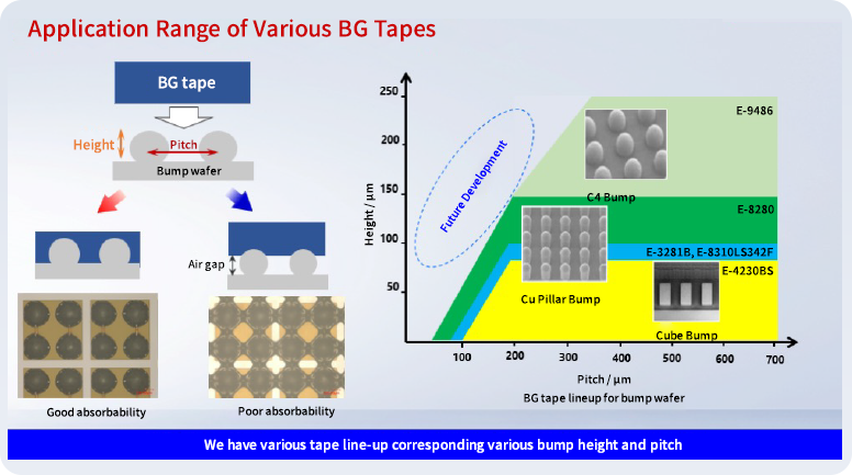
-Bump Wafer-
The indicated values are measured values and not intended for guarantee use.
| E-4230BS | E-3281B | E-8310LS342F | E-8280 | E-9486 | ||
|---|---|---|---|---|---|---|
| Tape Thickness(μm) | 230 | 280 | 310 | 280 | 485 | |
| Appearance | Blue | Blue | Blue | Blue | Transparent | |
| Structure | Base Film (μm) |
PO Composite Film 220 |
PET Composite Film 270 |
Special Elastomer 270 |
Special Elastomer 260 |
PET Composite Film 475 |
| Adhesive (μm) |
10 | 10 | 40 | 20 | 10 | |
| Adhesion*1 (mN/25 mm) |
Before UV | 4165 | 16600 | 7600 | 9200 | 13000 (2600)*3 |
| After UV*2 | 220 | 2800 | 270 | 480 | 1200 (240)*3 |
|
| Remark | For <80μm Bump |
For <100µm Bump for DBG™ |
For <100μm Bump |
For <150μm Bump |
For <250μm Bump for DBG™ |
|
*1: Peeling speed= 300 mm/min, Peeling angle= 180deg., Adherend: Si mirror wafer
*2: UV ray intensity: 230 mW/cm2, UV ray dosage: 550 mJ/cm2(For E-8310LS342F, E-8280 was 380 mJ/cm2 and E-9486 was 1120 mJ/cm2), Wavelength of ultraviolet should be around 365 nm.
*3: Peeling speed= 3000 mm/min, Peeling angle= 90deg., Adherend= Si mirror wafer
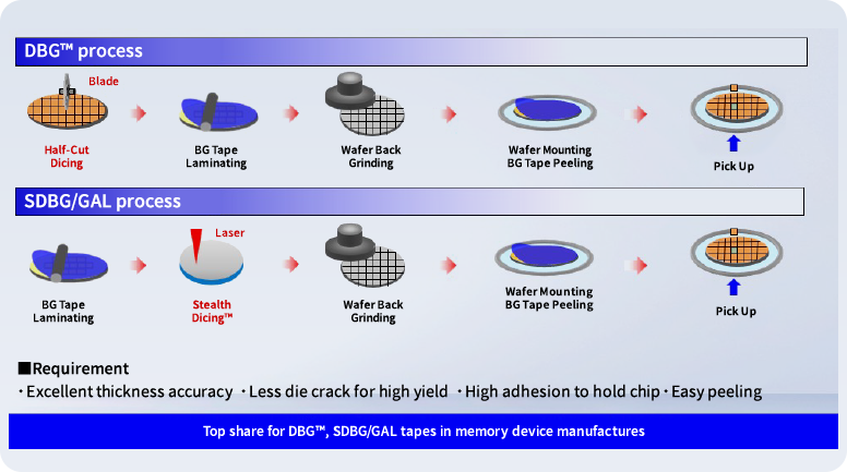
For Special Process
-DBG™, SDBG/GAL Process-
The indicated values are measured values and not intended for guarantee use.
| E-3125BN | E-3100UN | E-3090V | E-3100V | E-3140V | ||
|---|---|---|---|---|---|---|
| Tape Thickness(μm) | 125 | 100 | 90 | 100 | 140 | |
| Appearance | Blue | Blue | Blue | Blue | Blue | |
| Structure | Base Film (μm) |
PO Composite Film 105 |
PET Composite Film 80 |
PET Composite Film 80 |
PET Composite Film 80 |
PET Composite Film 80 |
| Adhesive (μm) |
20 | 20 | 10 | 20 | 60 | |
| Adhesion*1 (mN/25 mm) |
Before UV | 10780 | 13430 | 11500 | 12600 | 15600 |
| After UV*2 | 50 | 50 | 50 | 40 | 60 | |
| Remark | T.T.V. : Good | T.T.V. : Better | T.T.V. : Best | T.T.V. : Best | T.T.V. : Better | |
*1: Peeling speed= 300 mm/min, Peeling angle= 180deg., Adherend=Si mirror wafer
*2: UV ray intensity: 230 mW/cm2, UV ray dosage: 380 mJ/cm2, Wavelength of ultraviolet should be around 365 nm
For Special Process
-Chemical Etching-
The indicated values are measured values and not intended for guarantee use.
| E-3129R | E-4141A | E-6142S(S) | ||
|---|---|---|---|---|
| Tape Thickness(μm) | 120 | 140 | 130 | |
| Appearance | Blue | Opaque | Opaque | |
| Structure | Base Film (μm) |
PET Composite Film 80 |
PO 120 |
PO 110 |
| Adhesive (μm) |
40 | 20 | 20 | |
| Adhesion*1 (mN/25 mm) |
Before UV | 9800 | 3630 | 5400 |
| After UV*2 | 196 | 690 | 55 | |
*1: Peeling speed= 300 mm/min, Peeling angle= 180deg., Adherend=Si mirror wafer
*2: UV ray intensity: 230 mW/cm2, UV ray dosage: 380 mJ/cm2, Wavelength of ultraviolet should be around 365 nm.
*"DBG™" is trademark of LINTEC Corporation, Disco Corporation and KIOXIA Corporation.
"Stealth Dicing™" is trademark of Hamamatsu Photonics K.K.